
Laplanda IP_PS_012
Intragenomic Processor Rev.012 Ultra-Low-Noise 3 A Laser Diode Current Driver & High-Speed Waveform Controller
0–3 A Laser Current | 12 V Compliance | 5 ns Pulse Generation | <1 ns Measured Falling Edge | Battery Powered | Dual-Core STM32H747 Control
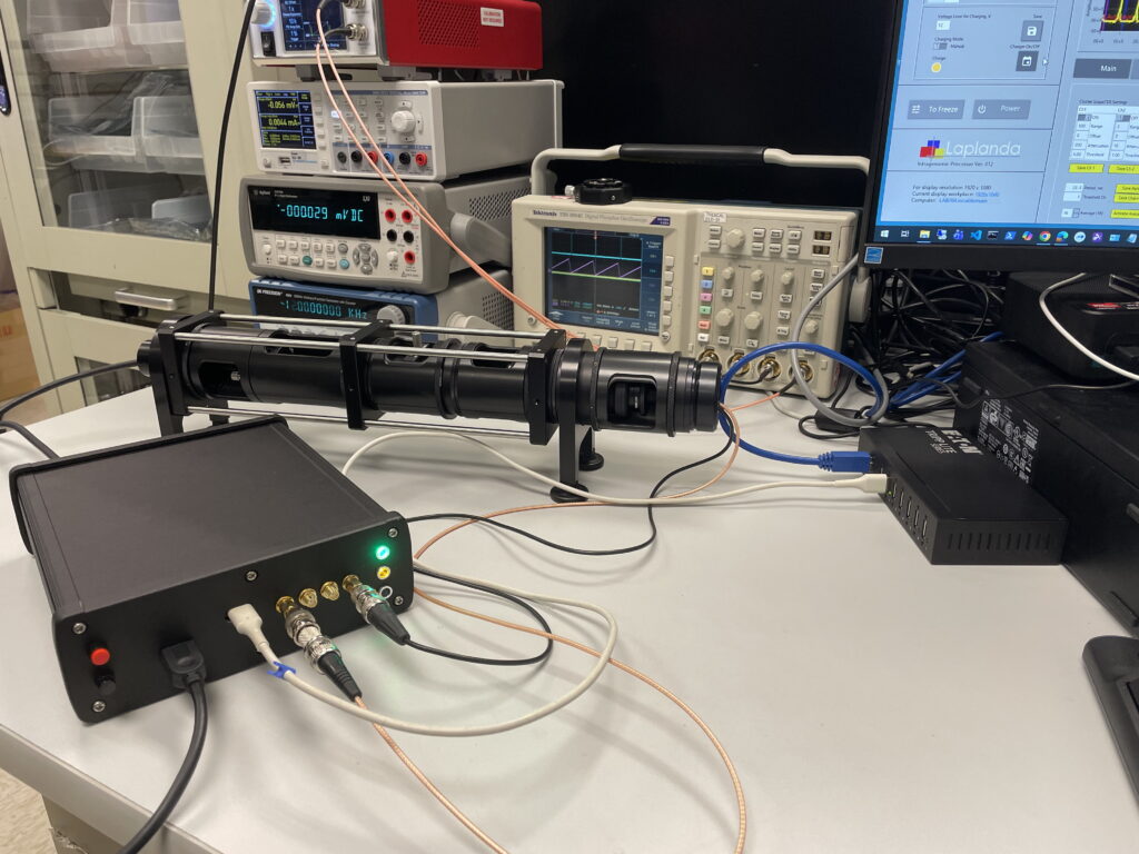
The Laplanda IP_PS_012 is an integrated ultra-low-noise laser-diode current driver, programmable waveform generator, high-speed pulse controller, and embedded control system developed for the Intragenomic Processor Rev.012.
Unlike a conventional laboratory laser-diode power supply, IP_PS_012 was designed to combine relatively high laser current with very fast electrical modulation. The system provides programmable laser-diode current up to 3 A, a maximum compliance voltage of 12 V, waveform generation, nanosecond pulse control, external triggering and acquisition interfaces, internal battery operation, and computer-based control within a single compact aluminum enclosure.
The architecture was developed specifically for experiments in which the laser is not simply operated continuously, but must become an actively controlled component of a synchronized measurement system.
Precision 0–3 A Laser-Diode Current Control
At the core of IP_PS_012 is a laser-diode current driver, rather than a conventional voltage-source output.
This distinction is important. Semiconductor laser diodes require controlled current operation because relatively small changes in junction voltage can produce large changes in laser current. IP_PS_012 therefore regulates and controls the laser drive while providing up to 12 V of available compliance voltage to accommodate the electrical requirements of the connected laser-diode system.
The Rev.012 controller supports laser-diode current operation from 0 to 3 A, substantially extending the capability of the earlier lower-current concepts considered during development.
High-Speed Waveform Generation
IP_PS_012 incorporates programmable waveform-generation capability for dynamic laser excitation.
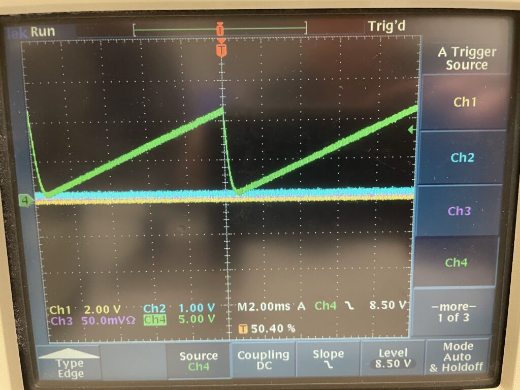
The demonstrated Rev.012 configuration generates a repeating sawtooth waveform with a 10 ms period, corresponding to a repetition rate of approximately 100 Hz. The available driver architecture operates with up to 12 V compliance, providing the electrical headroom required by the current-control stage.
The measured oscilloscope waveform in IMG_3215.jpg demonstrates the repetitive ramp and rapid reset behavior of the implemented controller.
This capability allows laser excitation to be varied continuously rather than simply switched between ON and OFF states, which can be useful for synchronized optical measurements, scanning experiments, characterization procedures, and specialized excitation sequences.
Nanosecond Pulse Generation
One of the principal features of IP_PS_012 is its high-speed pulse-control capability.
The completed controller provides pulse generation with a demonstrated minimum electrical pulse width of approximately:
5 ns
This timing capability is several orders of magnitude faster than the millisecond-scale waveform generator and allows the same instrument to support both relatively slow programmable excitation profiles and extremely fast laser-control events.
The high-speed section is deliberately separated conceptually from the MCU timing itself: the STM32H747 supervises and commands the instrument, while dedicated high-speed circuitry performs the nanosecond switching function. This architecture follows the design approach developed during the project specifically to avoid relying on general-purpose MCU GPIO timing alone for nanosecond laser switching.
Sub-Nanosecond Falling-Edge Performance
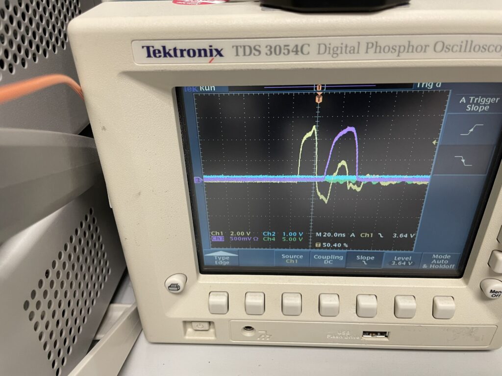
Testing of the completed Rev.012 hardware demonstrated an electrical falling edge of:
< 1 ns under the measured test configuration
This is an important distinction from the 5 ns minimum pulse width specification. Pulse width describes how long a generated pulse can be, whereas falling-edge time describes how rapidly the electrical drive transitions at pulse termination.
The oscilloscope capture shown in IMG_3213.jpg documents the measured high-speed switching behavior.
Because measured rise/fall times depend on test configuration, cabling, impedance, oscilloscope bandwidth, load, laser diode, and probing arrangement, I recommend publishing this specification as:
Measured electrical falling edge: <1 ns*
Measured on the Rev.012 prototype under the specified laboratory test configuration.
That wording is stronger technically than claiming an unconditional “<1 ns” specification for every possible load.
Ultrafast Optical Response Verification
Electrical switching speed alone does not establish the optical response of a semiconductor laser. For this reason, the Rev.012 development system was also evaluated optically.
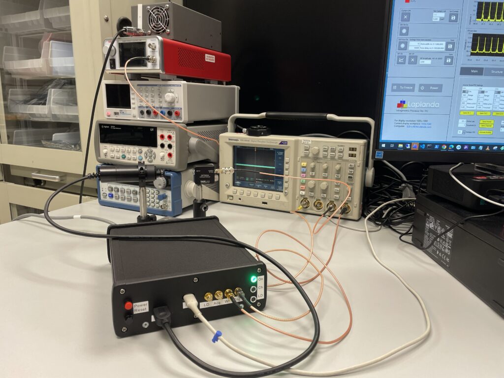
The laser output was measured using a Thorlabs DET025A ultrafast biased photodetector, visible in the test setup photographs.
The acquired waveform shown in IMG_3218.jpg demonstrates the temporal optical response of the laser beam to the high-speed electrical drive.
This measurement is particularly valuable for the product page because it demonstrates that development did not stop at observing an electrical signal at the driver output—the resulting optical behavior was also experimentally investigated.
The exact optical fall time should remain separate from the electrical <1 ns figure unless a calibrated bandwidth-corrected measurement establishes an optical number. Laser-diode carrier dynamics, detector response, interconnects, and measurement bandwidth can all affect the observed optical waveform.
External Signal Interfaces
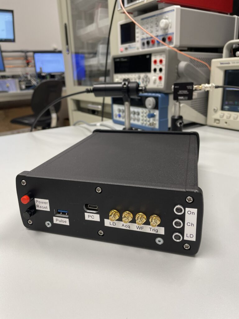
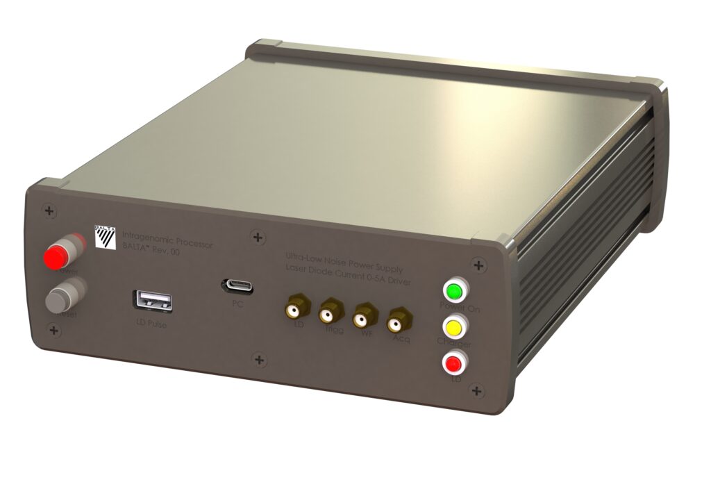
The front panel provides dedicated high-frequency connections labeled:
LD — Laser Diode
Acq — Acquisition
WF — Waveform
Trig — Trigger
These interfaces allow the controller to exchange timing and waveform information with oscilloscopes, acquisition electronics, detectors, external trigger sources, and other instrumentation.
Separating these signals onto dedicated connectors also makes IP_PS_012 particularly useful during experimental development because critical timing signals can be directly monitored with laboratory instrumentation.
The laboratory photographs demonstrate this configuration with the controller connected directly to the Tektronix oscilloscope and optical detector measurement system.
Dual-Core High-Performance Embedded Controller
The digital control architecture is based on the STM32H747XI, a dual-core 32-bit Arm microcontroller.
It incorporates:
| Processor | Performance |
|---|---|
| Arm Cortex-M7 | 480 MHz |
| Arm Cortex-M4 | 240 MHz |
| Architecture | Dual-core STM32H7 |
| Control role | Instrument management, waveform/pulse coordination, communications and real-time control |
The dual-core architecture is particularly useful for this type of instrument because computational, communication, GUI-interface, and supervisory tasks can be separated from timing-sensitive control functions.
The MCU therefore serves as the central control system while dedicated high-speed electronics handle events whose timing requirements exceed conventional software-controlled GPIO operation.
Laplanda PC Control Software
IP_PS_012 is designed as a digitally controlled laboratory instrument rather than only as a manually adjusted current source.
A dedicated customizable graphical user interface developed by Laplanda CC provides computer-based access to the controller.
The software architecture can provide centralized access to operating parameters such as laser operation, waveform configuration, timing, pulse functions, acquisition coordination, trigger control, and system status.
The front-panel PC USB-C connection provides the host-control interface.
This combination of embedded firmware and PC software allows the controller to become part of the larger Intragenomic Processor instrumentation environment instead of operating as an isolated laser driver.
Internal Battery Operation and Noise Isolation
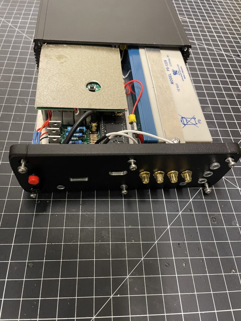
IP_PS_012 incorporates a self-contained 12 V, 2.9 Ah rechargeable battery system.
Battery operation is valuable for a precision laser controller because it provides a local DC energy source and can reduce direct coupling of AC-line disturbances into sensitive analog electronics during operation.
An integrated charging system automatically maintains the battery using predetermined upper and lower charging thresholds. This hysteretic charge-management strategy prevents the charging circuit from repeatedly toggling at a single threshold and allows automatic battery maintenance.
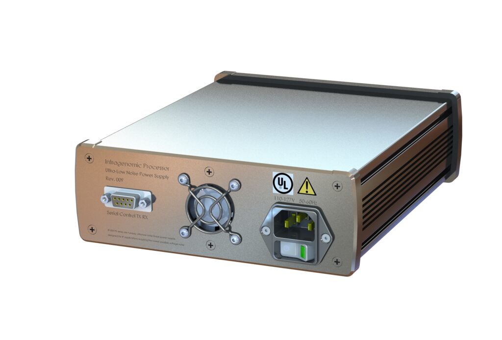
The rear panel incorporates an IEC AC power inlet and master power switch. The Rev.012 CAD marking indicates 110–127 VAC, 50–60 Hz operation for the present charger configuration.
Important Battery Documentation Correction
There is one item I recommend correcting before publishing the final website.
You described the installed battery as a 2.9 Ah lithium battery, but IMG_3209.jpg appears to show a 12 V PS-1229 battery carrying a Pb marking. That indicates a lead-based/sealed lead-acid battery, not a lithium battery.
Therefore, I would not publish “lithium battery” yet.
For now the commercially safe specification is:
Internal rechargeable battery: 12 V, 2.9 Ah
Once the exact production battery chemistry and part number are confirmed, the chemistry can be added to the specification.
Mechanical Construction
The controller is housed in a rigid aluminum electronics enclosure approximately:
7 in × 8.2 in × 2.4 in
or approximately:
178 × 208 × 61 mm
The aluminum construction provides a mechanically robust enclosure while also supporting shielding of the sensitive internal electronics.
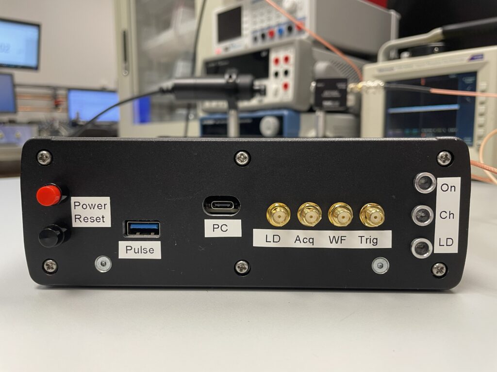
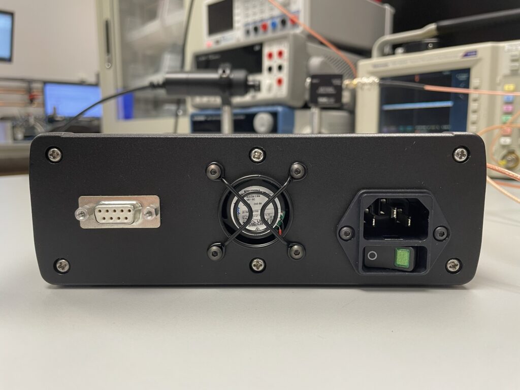
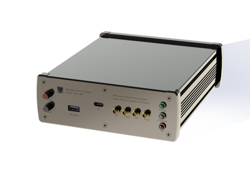
The front-panel arrangement separates control, computer, laser, waveform, acquisition, and trigger functions, while the rear panel contains the AC input, master switch, cooling fan, and serial/control interface.
The CAD design also provides a considerably more professional production appearance than the hand-labeled Rev.012 engineering prototype while preserving the tested connector arrangement.
| Parameter | IP_PS_012 Rev.012 |
|---|---|
| Product | Laplanda IP_PS_012 |
| Function | Ultra-low-noise laser-diode current driver and high-speed waveform controller |
| Laser current range | 0–3 A |
| Compliance voltage | Up to 12 V |
| Waveform capability | Programmable; sawtooth demonstrated |
| Demonstrated sawtooth period | 10 ms / approximately 100 Hz |
| Minimum demonstrated pulse width | ≈5 ns |
| Measured electrical falling edge | <1 ns* |
| Optical high-speed verification | Measured with Thorlabs DET025A |
| Main controller | STM32H747XI |
| High-performance core | Cortex-M7, 480 MHz |
| Real-time secondary core | Cortex-M4, 240 MHz |
| PC interface | USB-C |
| External interfaces | LD, Acq, WF, Trig |
| Software | Laplanda CC customizable control GUI |
| Internal battery | 12 V, 2.9 Ah rechargeable |
| Battery charging | Automatic hysteretic charge management |
| AC charger input | 110–127 VAC, 50–60 Hz for current Rev.012 configuration |
| Enclosure | Aluminum |
| Dimensions | 7 × 8.2 × 2.4 in |
| Approx. metric dimensions | 178 × 208 × 61 mm |
| Application platform | Intragenomic Processor Rev.012 |
| Development / Manufacturer | Laplanda CC |