Wafer HV Tester (WHVT)
The proof of the design is done in a conformance (type) testing: A high voltage is used to verify that the clearances and solid insulation of dies have adequate dielectric strength to resist expected overvoltage conditions. It also shows that the LED is able to work safely over its complete lifetime. During the test the electrical stress on the insulation over its complete lifetime is simulated in a very short time. Here it is assumed that the failure mechanism during lifetime is the same as in the test.
Typically the test voltage is calculated for an expected lifetime of 20 years. So equipment with an operating voltage of 230V has to be high voltage tested with a voltage of 3400V for one minute. This also means that the examined insulation is aged completely during the type test and cannot be used anymore.
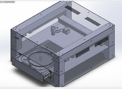
WHVT has a several basic components:
•Wafer loader,
•120 degree probe,
•Positioning station and
•Probe coordinate recognition
•Every component interfaced with communication software for ruling the test algorithm.
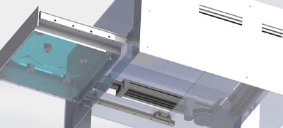
Machine vision system start the exploration of the Wafer for the coordinates for probe position.
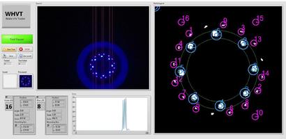
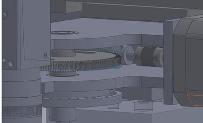
Upon the position for test is detected the probe is moving to the coordinates and at the time of positioning the nest magnets move the Wafer to Z vector for full electrical contact. When all 36 dies are contacted the test is started. The time for test is 1 sec. This time is enough to raise the voltage from 0 to 2000V with 250 kilosamples per second (16 bit word), that’s mean that 10 results per millisecond guaranty the high accuracy.